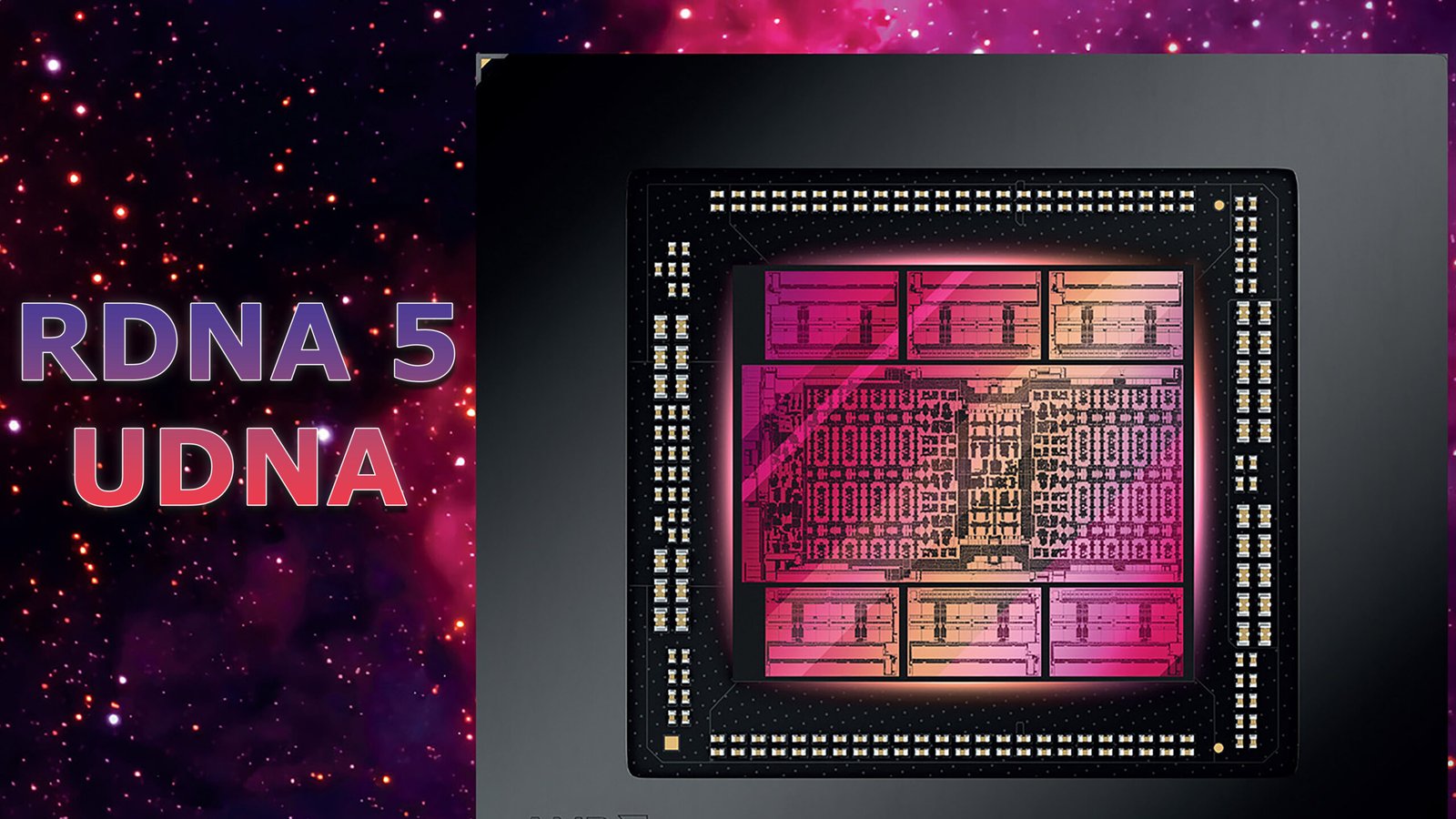
AMD’s next-generation GPU architecture, tentatively dubbed RDNA5 or UDNA, is shaping up to be a significant milestone for the Radeon family. According to insights from Kepler, a well-known hardware leaker with a strong track record in revealing GPU and console architecture details, RDNA5 is poised to deliver a comprehensive update targeting both gaming and AI workloads. This article explores the latest rumors and expectations surrounding this highly anticipated architecture.
The current RDNA4 architecture, powering the RX 9000 series, focuses on mid-range and high-end GPUs but lacks integrated or mobile variants. AMD scaled back its original ambitions for top-tier RDNA4 GPUs, opting for a more restrained lineup. However, this decision is expected to pave the way for a more robust RDNA5, which could include a true flagship GPU to challenge NVIDIA’s dominance in the enthusiast segment, currently led by NVIDIA’s AD102 and GB202 chips, which excel in both performance and memory capacity.
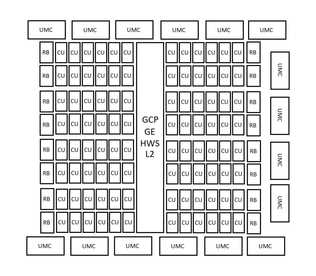
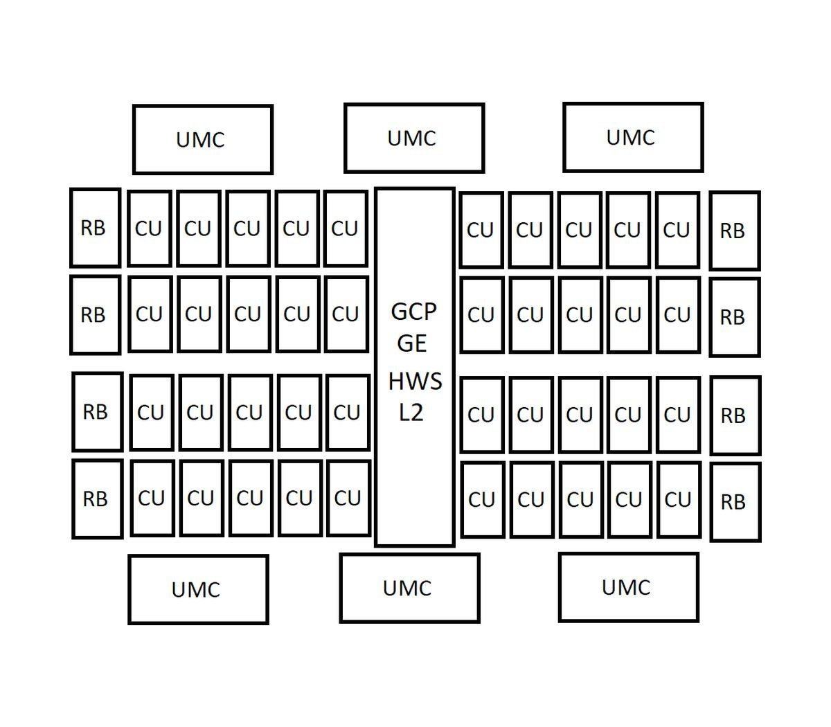
Source: Kepler
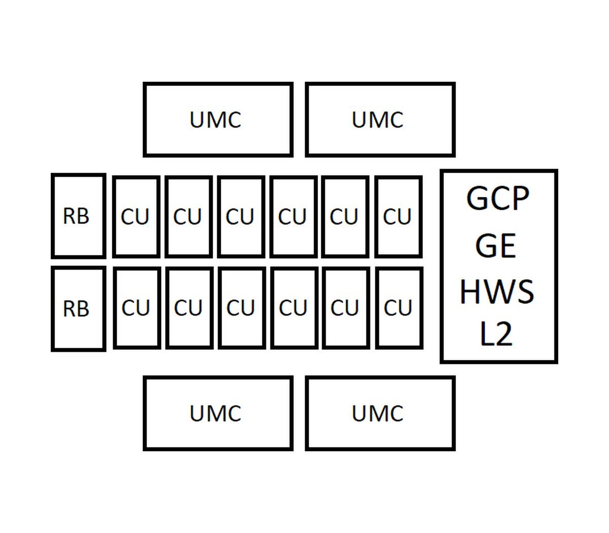
While concrete details remain scarce, early rumors about RDNA5’s flagship GPU, referred to as AT0, suggest a formidable design. The AT0 is speculated to feature 96 Compute Units (CUs) organized into 8 Shader Arrays, with each Shader Array housing 16 Shader Engines, and each Shader Engine containing 6 CUs. This configuration points to a powerful architecture capable of high computational throughput. Additionally, AT0 is rumored to utilize a 512-bit memory bus, which could significantly boost memory bandwidth compared to its predecessors.
A mid-tier GPU, dubbed AT2, is said to include 40 CUs, with each Shader Engine containing 5 CUs and a 192-bit memory bus supported by six Unified Memory Controllers (UMCs). Meanwhile, the AT3 and AT4 GPUs are expected to target lower performance tiers, with 24 and 12 CUs, respectively. Notably, AT3 may incorporate more UMCs than AT2, potentially due to its use of LPDDR5X memory, which requires additional memory controllers. Each memory controller is believed to be 16-bit wide, optimizing efficiency for these configurations.
The architecture’s design includes a Render Backend per Shader Engine, connected to the Graphics Command Processor (GPC), Graphics Engine, and L2 cache, ensuring streamlined data processing and rendering capabilities.
RDNA5, or UDNA as some sources call it, is expected to unify AMD’s approach to gaming and AI workloads. This dual-purpose design could position AMD to compete more effectively in both consumer and professional markets, leveraging advancements in compute performance and memory efficiency to cater to the growing demands of AI-driven applications alongside traditional gaming.
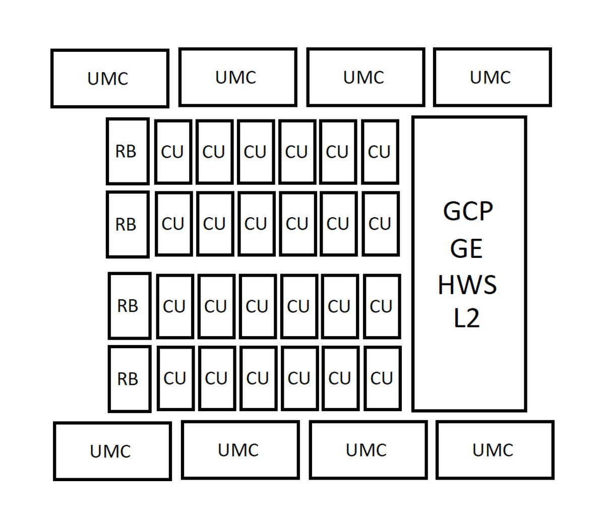
Source: Kepler
At this stage, speculation about SKU names or finalized specifications is premature. AMD may continue its current naming convention (e.g., Radeon RX 10700 or 10070) or introduce a new schema entirely, as the company has done in the past. More critically, there is no confirmation that AMD has taped out the silicon for RDNA5, meaning the final product lineup remains uncertain. Rumors about pricing or detailed specifications should be approached with skepticism until official announcements are made.
RDNA5 represents a bold step forward for AMD’s Radeon GPUs, with the potential to challenge NVIDIA’s lead in the high-end GPU market. By building on the lessons of RDNA4 and introducing a flagship GPU with robust compute and memory capabilities, AMD could redefine its position in the GPU landscape. As development progresses, enthusiasts and professionals alike will be watching closely for official details on this promising architecture.
Source: Kepler_L2

